Dzūkų str. 57-34, LT-02117 Vilnius, Lithuania
Tel. +370 5 212 26 91
Fax +370 5 212 26 92
E-mail:
Printable version of (none)
About Sapphire
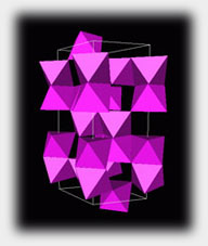
Fig.1.
Sapphire is single crystal — Aluminum Oxide (Al2O3) also known as α—Al2O3 which also includes Ruby (sapphire doped with Chromium). Sapphire is part of the larger class of Al2O3 crystals called Corundum. Sapphire has exceptional physical (optical, mechanical, dielectric and thermal) and chemical properties along with superior radiation stability when compared to other optical materials. For this reason sapphire is in high demand for many Scientific, Industrial and Military applications.
Using Crystallographic terminology, Sapphire crystals belong to the Rhombohedral class 3m system. Sapphire has the following symmetry elements:
inversion axis of 3nd order
3 axis of 2nd order which is perpendicular to inversion axis
3 planes of symmetry perpendicular to axis of 2nd order
center of symmetry
The Sapphire (corundum) structure can be represented by ordering octahedron is shown on Fig.1. O2- ions are in tops (peaks) of the octahedrons and Al3+ ions are inside of octahedrons.
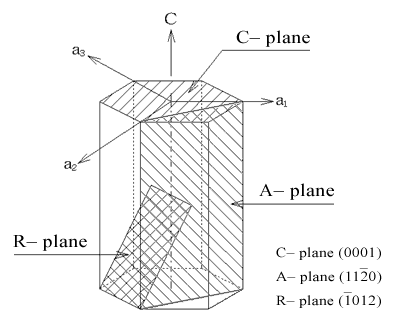
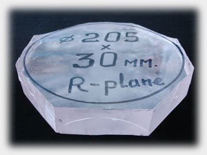
Fig.2 shows the structure of the primary planes of the sapphire crystal corresponding to the structure system of sapphire. Shown in this Figure, the C— plane is (0001), A— plane is (1120)and R— plane (1012).
Fig.2.
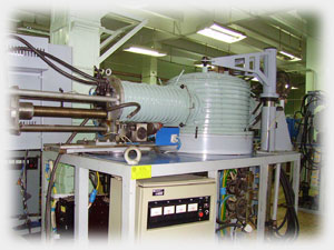
There are many different methods for growing sapphire. The most common are:
All of these methods have advantages and disadvantages, depending on the requirements.
The best optical quality sapphire can be achieved via the Bagdasarov , Czochralski and Kyropoulos methods. But in order to grow the high quality material from these methods, the growth rates are very slow. These methods yield the best sapphire for critical optical and semiconductor applications.
Stepanov method allows for faster, near-net shape growth such as plates, ribbon and tubes, saving considerable post growth processing. But the overall quality is not as good as Bagdasarov , Czochralski and Kyropoulos methods. In many applications such as display covers, scanner windows and watch crystals, Stepanov is more than adequate, at a much lower cost.
Verneuil is the “grandfather” of crystal growing, being the original method developed by professor Auguste Verneuil around 1902. Sapphire from the Verneuil method comes only in relatively small, round boules and is used mostly for mechanical applications such as bearings and wear parts but can also be used for low cost, small windows and for watching industry.
Some of the outstanding characteristics of sapphire:
Second only to diamond in hardness. Sapphire is extremely scratch and wear resistant. Combined with its excellent optical characteristics, sapphire is the ideal material for scanner windows, hazardous window applications and shields. It is also very useful in wear related non-optical applications such as bearings and nozzles.
Sapphire is transparent from 180 nm to over 5500 nm. This wide transparency window makes sapphire one the best materials in Optics and Micro Optics. In particular IR and UV systems. And because of its stability it is very resistant to optical damage such as solarization.
Sapphire has a high dielectric constant and low loss tangent, making sapphire an ideal material for semiconductor, electrical and microwave applications.
Thermal stability at very high temperatures (>1600C), far higher than any other optical material, and most non-optical materials. This makes sapphire ideal for semiconductor processing, Furnace applications and refining applications.
Exceptional chemical stability. The only chemicals that etch sapphire are molten salts. All other solvents, bases and acids do not affect sapphire, even at elevated temperatures. This makes sapphire ideal for high purity chemical processing, semiconductor processing and plasma systems.
Unlike glass, sapphire cannot be molded or melted into different shapes. To get near net shapes such as low tolerance tubes and ribbon, sapphire can be grown to that shape using the Stepanov method (EFG). But in most applications grinding and polishing with diamond is required. Diamond is the only media hard enough to process sapphire.
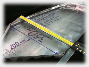
In addition, present day technologies are limited in how large the sapphire can be grown. The largest sapphire that can be produced is 300mm in diameter using the Kyropoulos (HEM) or Bagdasarov methods.
Sapphire Physical properties *)
Optical properties
Optical transmission range, µm
0.18 – 5.5
Refractive index at 0.532 µm
no = 1.7717, ne = 1.76355
Mechanical properties
Density g/cm3
3,97–3.99
Hardness
Mohs
Mohs
9
Knoop kg/mm2
||C 1525–1800
| C 1900–2100
Vickers (9.8N) GPa
||C 16-17
| C 18-20
Young’s modulus GPa
345–494
Tensile strength MPa
400
at 298K
275
at 770K
335
at 1000K
Compressive strength (Bulk modulus) GPa
2–2.9
Flexural strength GPa
||C 1.03
| C 1.54
compression modulus GPa
250
Rigidity modulus GPa
145–175
Repture modulus (MOR) MPa
350–690
Elasticity modulus N/mm2
3.6x10⁵
Poisson’s ratio
0.27–0.30
Jet abrasion resistance (acc. to Mackensen)
0.12 mm
Friction Coefficient
0.15 on Steel, 0.10 on Sapphire
Thermal characteristics
Melting point
2323 K (2050 °C)
Boiling point
3253 K (2980 °C)
Thermal expansion coefficient
(x10–6K–1)
293–323 K
||C 6.6
| C 5.0
310–670 K
||C 7.0
| C 7.7
1270 K
||C 9.03
| C 8.31
60 degr. to C-axis:
293-323
K 5.8
1270
K 8.4
1770
K 9.0
Thermal conductivity W/mK
30 K
10000
298 K
||C 32.5
| C 30.3
670 K
12.56
1500 K
4.0
Electrical characteristics
Resistivity Ωcm
293 K
||C
(1.2–2.9)x1019
| C
5x10¹⁸
573 K
1011
1270 K
109
1770 K
105
2270 K
103
Dielectric constant
293 K (20 °C)
| C 9.35
||C 11.53
370 K
| C 9.43
||C 11.66
570 K
| C 9.66
||C 12.07
770 K
| C 9.92
||C 12.54
970 K
| C 10.26
||C 13.18
293 K, 103–109 Hz
| C 9.3
||C 11.5
Dielectric tangent loss
293 K, 1010 Hz
||
C 8.610–5
|
C 3.010–5
Dielectric strength V/m
48x106
*) E.Dobrovinskaya, L.Lytvynov, V.Pischik “Sapphire in Science and Engineering”.